

Key Technology Opening the Glass Interposer Era: TGV Cu Plating and Bridge Filling Process
Key Summary
- Why Glass Substrates Are Attracting Attention: They are highly suitable for AI/HPC semiconductor packages due to low signal loss (Df ≤0.005), minimal thermal deformation, and low moisture absorption.
- Limitations of Conventional Plating: If the TGV entrance is blocked first, voids or seams may remain inside, reducing product reliability.
- Solution: A two-step process that first creates a Cu Bridge at the hole center using PPR (Periodic Pulse-Reverse), then fills remaining space with DC plating, is advantageous for defect-free filling.
Main Content
As AI and high-performance computing (HPC) advance, semiconductor packages require more signal lines packed into smaller spaces. Accordingly, Glass Interposers are emerging as a material to address the limitations of traditional organic and silicon substrates.
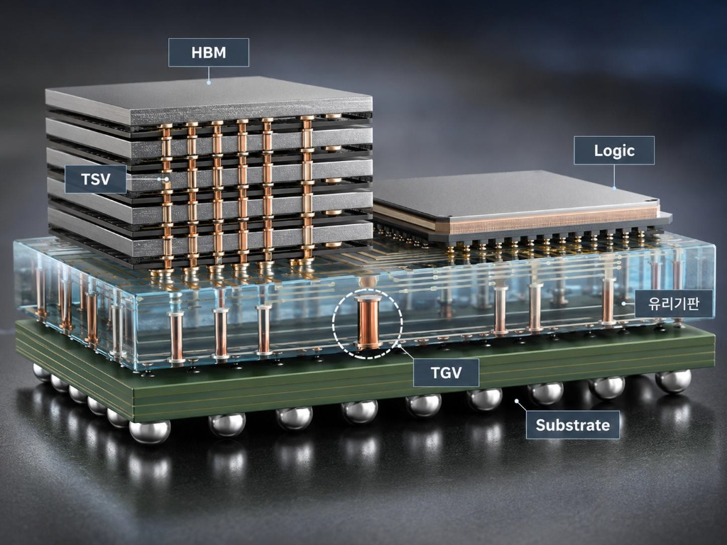
The Glass Interposer is a thin glass layer that connects signals between chips and substrates. The tiny via holes inside the glass, TGVs, are filled with copper to enable electrical signals to move vertically.
1. Why are Glass Substrates and Glass Interposers drawing attention?
HBM, Chiplet, 2.5D/3D packages require fast connection of many chips in a compact space. If the substrate warps from heat or signals weaken, performance and lifespan suffer. Glass substrates are smooth and thermally and moisture-stable, making them a promising next-generation high-performance packaging material.
| Category | Organic (Organic) | Silicon (Silicon) | Glass (Glass) |
| Surface roughness (nm) | 400~600 | ≤ 10 | ≤ 10 |
| Coefficient of thermal expansion (CTE, ppm/K) | 3~17 | 2.9~4.0 | 3~9 |
| Elastic modulus (Flexibility, GPa) | 10~40 | 165 | 50~90 |
| Moisture absorption rate (%) | 0.04 | 0 | 0 |
| Dielectric loss (Df) | 0.005~0.02 | 0.01~0.05 (Condition-dependent) | ≤ 0.005 |
| Typical substrate size (mm) | 415×510 | Ø300 | 415×510 , 515×510 |
Four Key Advantages of Glass Substrates
- ① Low signal loss (Df ≤0.005). : Less attenuation of high-frequency signals, making high-speed data transfer advantageous.
- ② Less deformation from heat (CTE 3~9 ppm/K). : Similar coefficient of thermal expansion as silicon chips, reducing warping or bending in large-area packaging.
- ③ Capable of producing large panels. : Enables wider rectangular panels compared to circular wafers, advantageous for productivity and cost.
- ④ Does not absorb moisture (0%). : Reduces deformation and electrical defects due to moisture, enhancing long-term reliability.
2. How to fill TGVs completely with copper?
TGV (Through-Glass Via) is a tiny hole penetrating through the glass substrate vertically. Filling it with copper allows signals to pass between chips.
Electrical signals can pass through.
However, standard DC (Direct Current) plating often results in rapid growth at the hole entrance, which can clog the entrance first, leaving voids or large seams inside, causing electrical and durability issues.
Main limitations of TGV filling methods
- ① DC plating: Can block the opening first, leading to large seams or voids.
- ② Conformal plating: Grows evenly on the walls but may leave gaps in the center.
- ③ Bottom-up plating: Suitable for unidirectional growth, but has limitations for through-holes that are open on both sides.
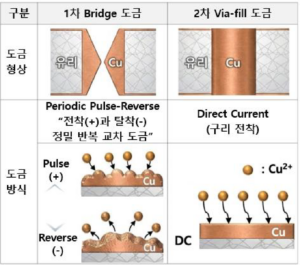
- ④ Bridge plating (our adopted method): Connecting the center first with a Cu Bridge, then filling the top and bottom spaces, is advantageous for void-free filling.
How does the Bridge method work?
- ① Suppress entrance growth: Uses inhibitors and reverse current to delay the premature closing of the entrance.
- ② Forming the center Bridge: Focuses copper growth at the center of the hole to connect the waist first.
- ③ Complete filling: Stabilizes the fill of top and bottom spaces based on the Center Bridge, reducing internal voids.
3. 2-Step process linking Bridge formation and complete filling
To fill TGVs seamlessly, the composition of the plating solution and the current waveform must be controlled together The key is to create a central bridge in the first step and reliably fill the remaining space in the second step
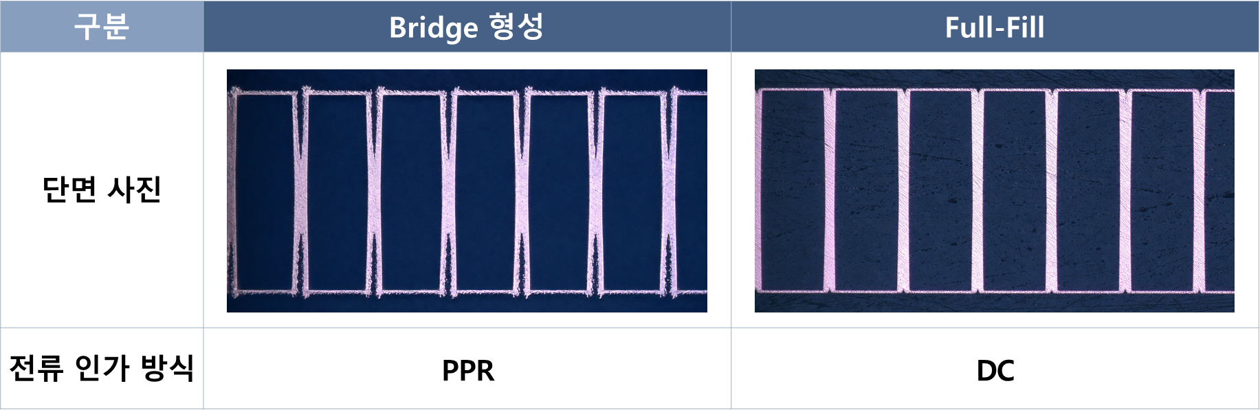
2-Step Plating Process
Step 1: Bridge plating (Bridge Step)
- Goal: First form a Cu Bridge at the hole center
- Method: Use PPR (Periodic Pulse-Reverse) that alternates between forward and reverse currents
- Effect: Suppresses excessive growth at the entrance and induces growth in the center
Step 2: Via-Fill plating (Fill Step)
- Goal: Fill the remaining space above and below the bridge with copper
- Method: Apply DC (Direct Current) or optimized current waveform
- Effect: Reduces internal voids and achieves a smooth surface finish (Leveling)
What role do additives in the plating solution play?
- ① Accelerator: Promotes copper deposition, accelerating growth at necessary locations
- ② Suppressor: Adsorbs strongly on the entrance surface, slowing copper growth to prevent early closure
- ③ Leveler: Selectively adsorbs on protruding copper surfaces to induce a uniform and smooth flatness
The balance of three additives and the PPR waveform must be optimized together to achieve stable Bridge and Full-Fill
4. Where is TGV Cu plating technology headed?
The key to commercializing Glass Interposers lies in defect-free, Void-Free copper filling of the TGV interior through advanced plating and process control technologies
Recently, research and technological innovation are focusing on the following technologies in the semiconductor packaging material and plating industries
- ① Filling deeper and narrower holes : Additives and processes are being developed to fill structures with an aspect ratio of 15:1 to 20:1, defined as depth divided by diameter, void-free
- ② Shortening plating time : Researching waveforms that combine PPR and DC to prevent entrance closure while increasing current density, and developing high-current additives
- ③ Customized filling processes based on via shape : A flexible 2-Step plating process library, adjusting bridge position and current conditions based on hole shape such as Hourglass, Straight, Tapered, etc., is being developed : Is being established
- ④ Improving environmental performance and lifespan : Moving towards reducing additive decomposition by-products and increasing plating solution exchange cycles to lower wastewater and operational costs
Our company is optimizing plating solution composition and current waveforms together, developing solutions that support defect-free filling and mass production in various TGV structures, and leading sustainable growth in the next-generation semiconductor packaging market beyond simple performance to environmentally friendly, long-life (Long Bath Life) plating solutions that minimize additive decomposition by-products