Thin film materials
Material properties decide display performance.
At LT Metal, we push that precisionone step further every day.
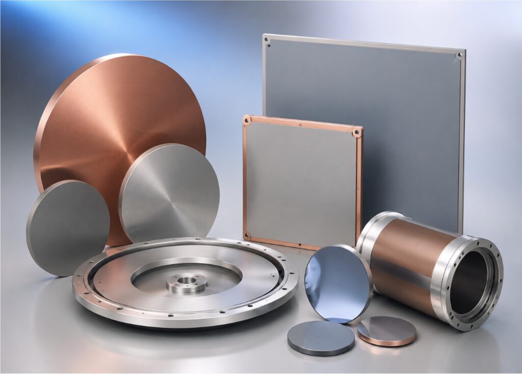
Thin-film materials form functional metal layers from a few nanometers to a few micrometers thick, deposited by sputtering or evaporation. The purity, density, crystal structure, and compositional uniformity of the target directly determine the electrical and optical properties of the film. Across semiconductors, displays, solar cells, and medical devices, thin-film material quality determines both product performance and manufacturing stability. LT Metal brought ITO target production to Korea with its own powder synthesis technology. Building on years of metal alloy expertise, we deliver consistent quality and stable performance in both ceramic and metal targets.
Process Selection Guide
Sputtering vs. Evaporation – Optimal Materials by Process
| Process | Requirements | LT Metal Materials | Main Applications |
|---|---|---|---|
| Sputtering | Large-area uniformity, low particle High purity, high density Low resistance, etchability·high adhesion High transmittance, high reflectance |
Pure metal and alloy targets Ceramic targets Hybrid targets |
TFT gate, S/D interconnects Buffer, diffusion barrier, capping layer Active layer, transparent electrodes OLED anode cathode Low-reflection and high-reflection films |
| Evaporation | High purity, low gas content | Ag(Disk, Pellet, Granule) Pt Pellet |
OLED Cathode R&D use |
Display vs. Semiconductor vs. Solar – Optimal Materials by Industry
| Industry | Requirements | LT Metal Materials | Main Applications |
|---|---|---|---|
| Display | Large-area uniformity, low particle High purity, high density, low gas content Low resistance, etchability·high adhesion High transmittance, high reflectance |
Pure metal and alloy targets Ceramic targets Hybrid targets |
TFT gate, S/D interconnects Buffer, diffusion barrier, capping layer Active layer, transparent electrodes OLED anode cathode Low-reflection and high-reflection films R&D use |
| Semiconductor | High purity, low gas content Large-area uniformity, low particle Grain control |
Pure metal and alloy targets | Interconnects, barrier, diffusion prevention Bumping EMI-Shield R&D use |
| Solar | Large-area uniformity, low particle High purity, high density High mobility, low resistance, high transmittance |
Ceramic targets Pure metal targets |
Crystalline Si TCO layers Electrodes and seed layers |
Product lineup
· Packaging: +82-32-820-9694
· Thin-film: +82-32-820-9694
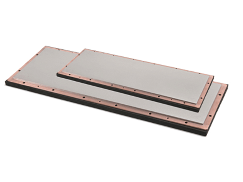
Ceramic Target
ITO, IZO (FPD·touch panels·solar) / IGZO, ITZO (OLED oxide TFT) targets supplied in planar/rotary types.
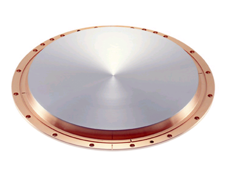
Metal Target
High-purity pure metal / alloy targets for FPD · touch panels · solar, supplied in planar/rotary types.
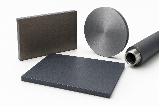
Hybrid Target
Metal–ceramic composite Mo/W-based (low-reflection) targets supplied in planar/rotary types.
Why LT Metal
Three engineering capabilities
Global customers choose LT Metal because our engineering capability in composition, structure, and reliability delivers the performance and quality they specify. That is our core strength.

We engineer composition.
The alloy composition and impurity level of a target directly determine the electrical and optical properties of the film. LT Metal analyzes your deposition conditions — temperature, pressure, and power density — and engineers a target with the composition to match.

We engineer structure.
Our proprietary technology synthesizes the powders for ITO and other functional targets in-house, so particle size distribution, oxygen content, and sintered density are engineered from the start. The result is a target structure that suppresses particle generation and arcing.

We engineer reliability.
We do more than supply material. We engineer a reliability support system around your deposition process: process condition reviews, prototype evaluation, and root-cause analysis when problems arise.