

Semiconductor Sputtering Targets: Process-Specific Applications and Core Design Technologies
Executive Summary
- Principles and Characteristics of the Sputtering Process : A core physical vapor deposition (PVD) technique where plasma ions collide with a target to form nano- scale, thin, and uniform films.
- Key Sputtering Target Applications by Semiconductor Process : Utilization of diverse materials tailored to specific process characteristics, including metal interconnects (Cu, Al) and diffusion barriers (Ta, Ti).
- Core Factors Determining Target Performance: High purity, high density, and microstructural grain control technologies are essential to enable high-quality film formation and yield enhancement.
What is the Sputtering Process?
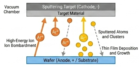
The sputtering process is a type of Physical Vapor Deposition (PVD) method used in semiconductor manufacturing to deposit thin, uniform metallic or insulating films onto wafer surfaces. To understand its role simply: for the semiconductor chips embedded in essential everyday electronics like smartphones and computers to function, they require microscopic electrical circuits (interconnects). The sputtering process can be thought of as laying down a thin canvas (the thin film) upon which these circuits can be drawn. Inside a vacuum chamber, an inert gas (primarily Argon, Ar) is pressurized with high voltage to transition into a plasma state. The positively ionized argon ions then vigorously collide with the surface of the ‘Target’ material, which is connected to a negative (-) cathode. During this impact, atoms from the target surface are ejected (sputtered) and deposit onto the opposing wafer (substrate), forming a thin film. To use an everyday analogy, the mechanism is highly similar to a game of billiards, where the cue ball (argon ion) forcefully strikes the object balls (target atoms) to drive them toward a specific target location (the wafer).
Types and Characteristics of Sputtering Processes
Sputtering processes are broadly classified into three major categories based on the applied power source and the utilization of magnetic fields. Each process is selected according to the target thin-film material and the specific application objectives.
DC Sputtering (Direct Current Sputtering)
This is the most fundamental and straightforward method that utilizes a direct current (DC) power source. It features a simple system configuration and a fast deposition rate, making it widely used for depositing metallic (conductive) thin films such as aluminum (Al) or copper (Cu). However, when a target made of an insulating material (non-conductive) is used, positive charges accumulate on the target surface, causing the plasma discharge to cease. Consequently, this method is strictly limited to conductive materials.
RF Sputtering (Radio Frequency Sputtering)
This method alternates and applies a radio frequency (RF) power source to prevent the accumulation of electrical charges on the target surface. It features high versatility, enabling the deposition of insulating targets—such as oxides and nitrides—in addition to metals. However, because electrons oscillate back and forth and lose energy in the process, it has the disadvantage of a relatively slower deposition rate compared to DC sputtering.
Magnetron Sputtering
This advanced method establishes a magnetic field inside the vacuum chamber by positioning powerful magnets behind the sputtering target. The magnetic field traps electrons around the target, significantly increasing the local plasma density, which exponentially accelerates the collision frequency of ions. As a result, the deposition rate is drastically improved, and high-quality thin films can be formed even at low vacuum levels and low temperatures. This technique has firmly established itself as a core process in modern mass-production lines for semiconductors.
Sputtering Target Applications by Semiconductor Process
As semiconductor chips become increasingly high-performance and circuit line widths shrink down to the nanometer (nm) scale, sputtering target materials have also become highly advanced and precisely tailored to the specific objectives of each process.
Metal Interconnect Process (Metalization): Cu, Al Targets
This process lays down the “microscopic highways” that connect billions of transistors within a semiconductor chip to enable electrical conductivity. In the past, aluminum (Al) targets were predominantly used due to their excellent adhesion to silicon and ease of processing. However, as processes have scaled down, reducing interconnect resistance has become critical. Today, copper (Cu) targets—which offer lower electrical resistance than aluminum and superior resistance to electromigration (EM), preventing circuit breakage—are utilized as the core interconnect material for high-performance semiconductors.
Diffusion Barriers & Barrier Metals: Ta, Ti Targets
While copper (Cu) exhibits excellent electrical conductivity, it possesses a fatal flaw: it easily diffuses (migrates) into the underlying silicon or insulating layers of the semiconductor. If copper diffuses into these regions, it causes malfunctions or catastrophic failure of the semiconductor device. To prevent this, a thin protective layer is deposited on the trench walls before forming the copper interconnects, a process that utilizes tantalum (Ta) or titanium (Ti) targets. These materials act as a robust barrier preventing copper penetration, thereby ensuring the long-term reliability and lifespan of the chip.
Core Factors Determining Sputtering Target Performance
A sputtering target used for semiconductor manufacturing is not a simple block of metal. Because it is a cutting-edge component that dictates semiconductor yield and thin-film quality, precise design and quality control during the manufacturing process are mandatory.
High Purity
In ultra-fine, sub-nanometer fabrication processes, impurities as minuscule as 1 ppm (parts per million) directly trigger circuit short circuits or chip defects. Therefore, sputtering targets for semiconductors must maintain an ultra-high purity level of 99.999% (5N) to 99.9999% (6N) or higher. The presence of mixed impurities leads to irregular electrical resistance within the thin film or introduces catastrophic defects into the device structure.
Density and Internal Pore Control
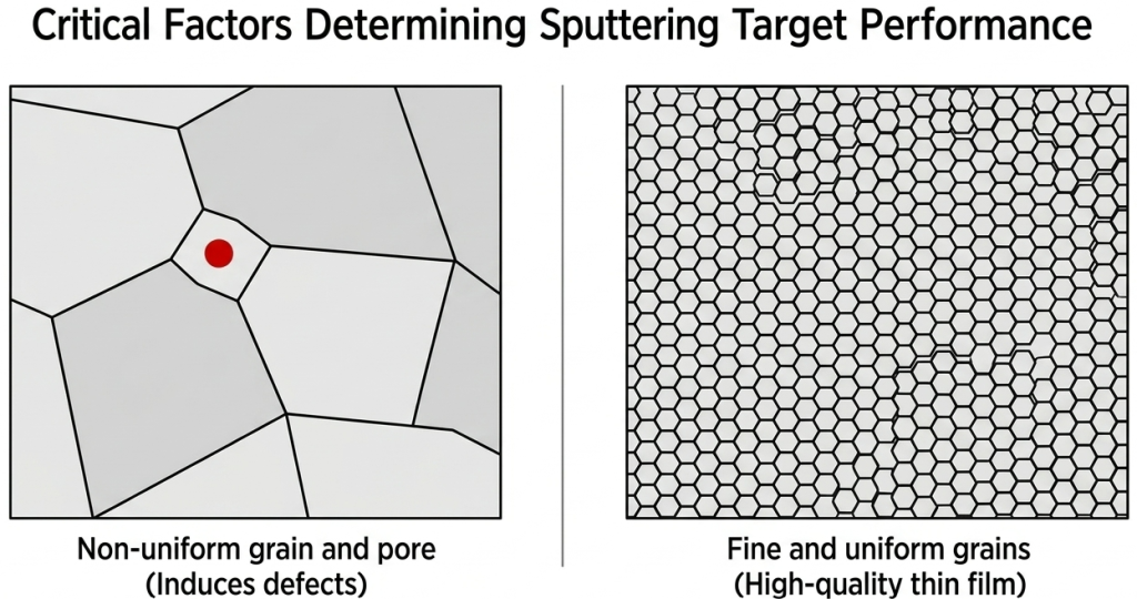
If empty spaces (pores or voids) exist inside the target material, trapped gases can abruptly erupt during the sputtering process, or target fragments can detach en masse. This material shedding forms particles (contaminating particles) on the wafer surface. To prevent this, the target must be manufactured via specialized heat treatment and compression processes to tightly compact the material close to 100% of its theoretical density.
Grain Size and Uniformity
As the size of the metallic crystalline grains composing the target becomes smaller and their crystalline orientation becomes more aligned, the ejection velocity and trajectories of the sputtered atoms become uniform. This plays a decisive role in forming a thin film with exceptionally homogeneous thickness and physical properties across the entire surface area of the wafer.
Latest Technology Trends in Semiconductor Sputtering Targets
With the recent advancements in Artificial Intelligence (AI) and High-Performance Computing (HPC), the introduction of sub-3nm ultra-fine fabrication processes and 3D advanced packaging technologies—such as High Bandwidth Memory (HBM)—has led to increasingly stringent requirements for sputtering targets. Going beyond conventional single metals, research into next-generation sub-nanometer interconnect materials, including Cobalt (Co) and Ruthenium (Ru), is highly active, driving a surge in demand for novel alloy targets. Furthermore, “high-efficiency, long-lifespan target designs” engineered for extended operational cycles upon installation, alongside eco-friendly resource recycling technologies that reclaim precious metals from spent targets to reuse them as high-purity raw materials, have established themselves as vital industrial trends.
The Value of Target Materials: Perfected through Design and Implementation
The quality of a sputtering target serves as the most fundamental and critical foundation determining semiconductor yield and device performance. Advanced metallurgical expertise to manage extreme purity levels and perfectly control nano-scale fine grains, combined with mass-production stability for consistent large-scale manufacturing, constitutes the core competitiveness of a target manufacturer.
Moving forward, continuously breaking through the physical limits of semiconductor scaling will require sustained research and development (R&D) in next-generation target materials aligned with evolving thin-film processes. This ongoing innovation will ultimately serve as the core driving force leading the future of semiconductor technology.
FAQ (Frequently Asked Questions)
Q1. What is a sputtering target?
It refers to a block of metal, alloy, or ceramic that serves as the raw material when depositing a thin film onto the surface of a semiconductor wafer. Inside a vacuum chamber, plasma ions collide with this target, causing atoms from the target to be ejected and subsequently deposited onto the wafer surface.
Q2. What is the reason for using copper (Cu) instead of aluminum (Al) in the metal interconnect process?
Copper has a significantly lower electrical resistance than aluminum, which greatly enhances signal propagation speed. Furthermore, it possesses superior resistance to electromigration (EM)—a phenomenon where moving electrons degrade and sever the interconnect lines—making it far more advantageous for advanced processes that require patterning ultra-thin and fine circuits.
Q3. Why are diffusion barriers (barrier metals) necessary?
They are required to prevent interconnect materials like copper (Cu) from diffusing into the silicon substrate or insulating layers, which can cause electrical shorts and device failure. Titanium (Ti) or tantalum (Ta) targets are primarily used to deposit a thin protective barrier that encapsulates the copper lines.
Q4. What factors determine the quality of a sputtering target?
The core elements are ‘ultra-high purity (minimizing impurities),’ ‘high density (minimizing internal voids/pores),’ and ‘grain size and uniformity.’ These parameters are critical factors that dictate the thickness uniformity of the deposited thin film and determine whether defects (particles) will occur.
Q5. Is recycling technology applied to sputtering targets as well?
Yes, it is. Expensive target materials remaining after semiconductor processing—such as copper, titanium, tantalum, and precious metals—undergo specialized purification processes to completely eliminate impurities. They are then regenerated into ultra-high purity raw materials of 99.999% (5N) or higher, contributing to environmental protection and cost reduction.